|
Labtool-T400 Software version 4.0 has make big progress in NAND flash support |
| Following is the major features and improvement |
| |
|
|
1. |
Speed improvement in Erase, Blank Check ,Program, Verify |
| |
Following is the speed compare between the SW 4.0 and previous version in detail |
| |
 |
| |
Note1: |
| |
The SW 4.0 perform program the entire block then verify the entire block after program, the default setting has change to program and verify only, customer can't setting the program and verify then verify simultaneously, no separate verify after program is required. this will also reduce the time too, in this 2G large block NAND flash, it take 202.54sec to program and verify the whole 2G chip compare to the old version SW m it take 558.43 sec, the speed is 2.7 times then the previous SW version, in another word the throughput is 2.7 time then before. |
| |
 |
| |
Note2: |
| |
SW 4.0 has change the default setting in NAND flash, only program and verify is requires, it don't need an extra verify after program the chip, the total time require to program whole 512M bit NAND flash is only 78.75 sec compare to the old version software, it takes 156.12 sec, the speed is 2 time and has 200 % throughput then before. |
| |
|
|
2. |
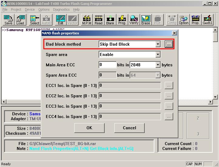
Skip bad block become a default setting after select the NAND flash chip. |
| |
 |
| |
In previous SW software (SW 3.62 and before), the default setting is None, when select the skip bad block, user need to edit the Start block , Last block , Total block by himself, if the user do not edit this value and using the default value, it means the setting is equal to setting at none (not allow any bad block and if any bad block found, it return program error or error message not enough good block) this setting created lots of support issue, in this SW V4.0 we change the default to Skip bad block. and the start block, last block, total block is not allow user to edit directly, to change this block setting, user has to go one step further to set the NAND flash partition screen then edit each partition and its start/last block, total block, then this partition set up will automatic change and fill those block data into the device option screen. |
| |
|
|
3. |
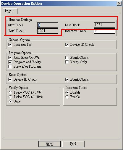
Automatic setting the start block, last block and total block with Max bad block in the chip datasheet. |
| |
 |
| |
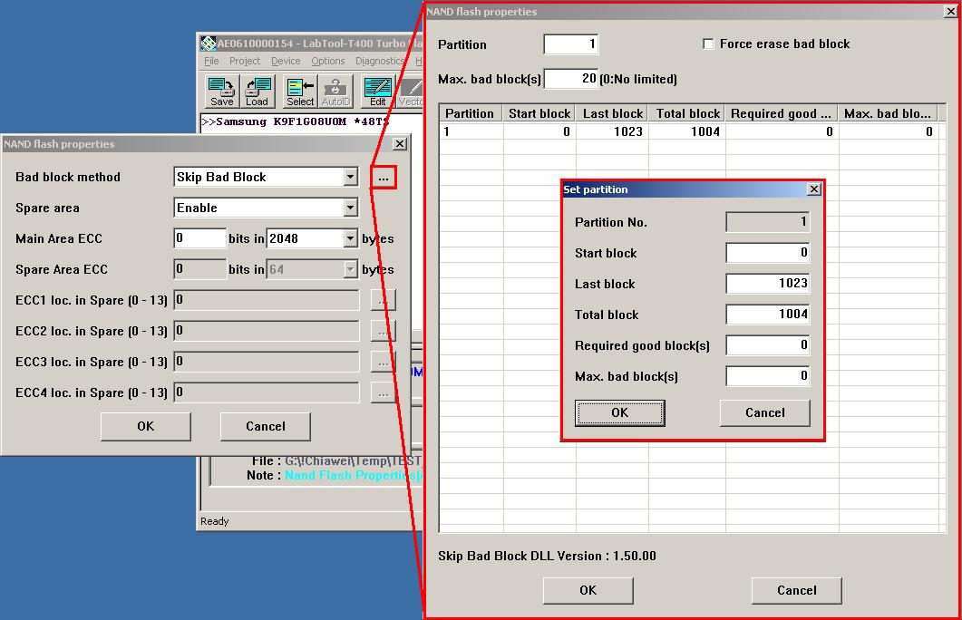
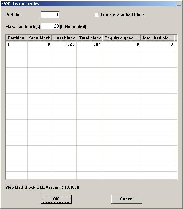
In the Skip bad block set up, the SW 4.0 has automatic setting the Start Block to 0, Last Block (chip's last block) and the total blocks change to the minimum good block in the chip guarantee by the chip vender. For example when select a K9F1G08U0M the start block will be 0 and last block will setting to 1023, the total block will be setting to 20 bad block Max, the total block now equal to 1024-20=1004. |
| |
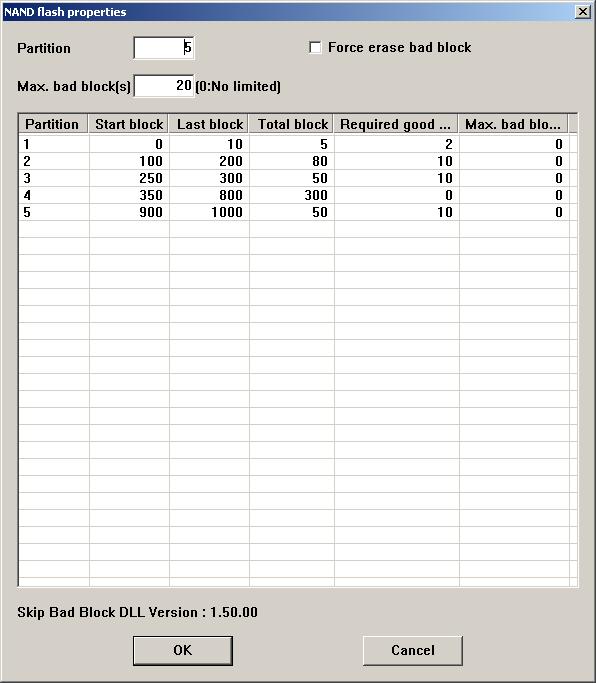
To change this start block. last block and total block. user need to go to the following partition screen to set the NAND flash partition and start block, last block and total block...etc |
| |
 |
| |
|
|
4. |
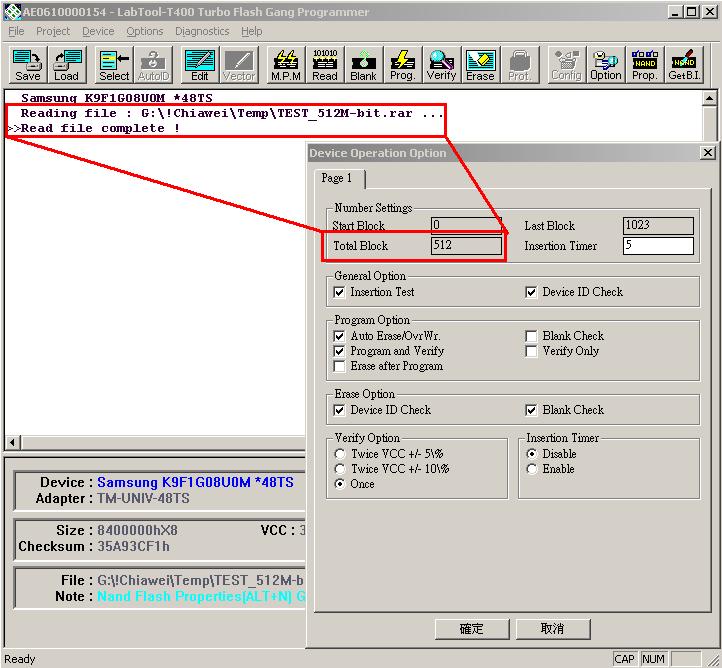
Detect the loading file size and automatically setting the total block size. |
| |
 |
| |
This feature allow the user to load the file without set up the partition one (default one partition only), the SW will calculate this file size and determined how many block required to fit this file. Then it automatically change the total block size, with his feature no other setting block size is required, it eliminate the mistake from the operator to setting and NAND flash property manually. It also speed up the programming time since the un-use block is skip when program and verify. |
| |
|
|
5. |
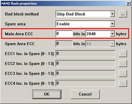
Main Area ECC function |
| |
 |
| |
This feature allow the user to setting one bit ECC error on 1 page or any specific byte (256 byte, 512 byte or 1024 byte) when enable this function, if a chip has 1 bit error in this range, the SW will continuous the program and verify process and no return any error message, If two or more bit error been found during program and verify, it will mark as bad block and skip it, when 0 bit ECC been selected, it means any bit error in the select area will mark as bad block and skip. |
| |
In this SW 4.0 release, we only provide 1 bit main ECC error function; future software version will add multiple ECC bit error function when the multiple bit error ECC is request. |
| |
This new ECC feature is reserved for future Multi-level cell chip with high density and has multiple bit error in one page. |
| |
Futures CPU power and software may able to correct multiple ECC error and usge those high no bit error chip. |
| |
|
|
6. |
New Save/load define file for NAND flash Partition set up. |
| |
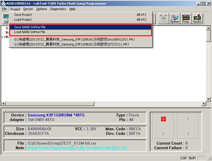
In this SW 4.0 we offer a new load/save function, file name xxxx.NSF |
| |
 |
| |
Following figure is an example show the default setting in NAND flash partition when select a NAND flash, if the user has create A xxxx.NSF file and save it, user can load this NSF file and the NAND flash partition will change according to the file. |
| |
This features more flexibility in the NAND flash set up, user don't need to set the partition when change to 2nd source chip. |
| |
 |
 |
| |
|
|
7. |
Change the default device operation option screen |
| |
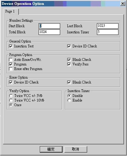
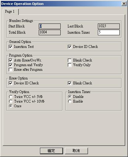
From the following screen you can find the major different in the SW 4.0 and previous SW version is option set up |
| |
SW 3.6 device operation option |
SW 4.0 device operation option |
| |
 |
 |
| |
The Number setting is different (reference to item 3), the total block is change to total block to minimum bad block, in this example 1024 to 1004, to change this No, you need to set up the partition screen or load xxx.NSF file, it cannot edit this no from the device option screen. |
| |
The Program option is change from enable (program, blank check, verify pass) to enable (Auto Erase/OvrWr., program and verify) verify pass change to verify only, user can't enable the program and verify simultaneously, Auto erase became default since chip vender recommend to erase the chip first and skip the blank check, program each block then verify the block is enough in NAND flash, do not need to verify whole chip after program, this will save lot of time in production, verify only is for QC to check the chip after program the whole batch then sampling check if the chip been program correctly. |
| |
|
|
8. |
Large NAND flash support, support 8 G bit, 16 G bit, 32 G bit with 4G bit buffer size. |
| |
Which means customer can select 8G/16G/32G bit device and program 4 G bit size ( select any block range that don't exceed 4 G size) , for customer who need for then 4G buffer size need to contact AEC to get special software release at charge.
|